
The OpenPOWER Foundation enables organizations worldwide to build, deploy, and innovate on the POWER platform — an open, royalty-free architecture with native AI acceleration, proven reliability, and a global ecosystem of hardware, software, and expertise.
When your workload is regulated, mission-critical, or classified — you cannot outsource your compute stack to a foreign vendor's cloud. POWER gives you AI performance, memory scale, and hardware isolation entirely within your own infrastructure.
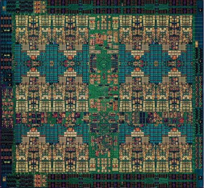
The Matrix Math Accelerator (MMA) is built directly into the POWER ISA — not a bolt-on GPU. Run LLM inference, fraud detection, and medical imaging models on your own hardware, inside your security boundary. Patient records and trading data never leave your data centre to reach an AI API.
ISA Specification →A 70B-parameter model requires ~140 GB of memory just to load — and conventional DIMM slots hit a hard ceiling. The Open Memory Interface (OMI) lets you scale memory capacity and bandwidth independently of the CPU, at DDR5 speeds, using hardware from any vendor. No proprietary memory bus, no single-source dependency.
OMI Specification →Osmosis connects FPGAs, HSMs, and AI accelerators directly to the POWER processor memory fabric with coherent, zero-copy bandwidth — eliminating the latency and overhead of conventional accelerator buses. The specifications are publicly archived. FPGA reference designs are live on GitHub. The initiative is advancing patent license grants from the original consortium founders to make the full stack freely deployable by OPF members.
Support this initiative →POWER's Logical Partitioning (LPAR) is defined in the ISA itself — not a hypervisor policy. A trading system and a compliance engine on the same physical server are cryptographically separated at the processor level. Each partition has its own privilege domain, memory protection, and interrupt handling, enforced by the architecture. This is how POWER runs in central banks, payment networks, and classified government systems.
Technical Overview →POWER is the architecture of choice when the workload is enterprise AI, mission-critical data, or production data center infrastructure — open by design, proven at scale, and ready today.
AI has reshaped the compute landscape. POWER's open architecture and MMA instructions give developers and enterprises the freedom to optimize at every layer of the stack.
Mission-critical HPC requires a portable, production-ready stack. POWER delivers proven performance for scientific computing, financial modeling, and real-time analytics.
With a royalty-free ISA and a growing global membership, OpenPOWER is the only open architecture with a full enterprise software and hardware ecosystem ready for deployment today.
Decades of investment in POWER hardware, open firmware, and software mean you can deploy with confidence — no waiting for ecosystem maturity.
Whether you ship products on POWER today or want to start, there's a path for you — from co-developing next-generation silicon to deploying production infrastructure.
Extend your POWER infrastructure investment into the next generation. Access the Silicon Factory's AI-powered chip development pipeline and early silicon programs.
A royalty-free, open architecture with decades of production validation. Hyperscalers get a differentiated silicon path — UCIe chiplet interfaces, POWER ISA reference IP, and IBM patent coverage for compliant implementations.
Design OCP-compliant servers and accelerator trays with a fully open ISA at the core. No per-unit royalties, fully auditable firmware — and a growing community of operators who already buy POWER-based infrastructure.
Start from open-source synthesizable POWER ISA cores (Microwatt, A2I, A2O). You get a production-proven ISA without royalty entanglement or vendor dependency.
Not sure which track fits? Start here.
Talk to the OpenPOWER team →The open commons every POWER implementation builds on — synthesizable cores, firmware stacks, and active ISA development. Free to all, governed by the community. View all open source →
A fully open source, synthesizable POWER ISA soft-core that runs Linux on FPGA — and has been taped out as a real ASIC via the OpenROAD toolchain. The reference implementation for the open POWER ISA.
An open source out-of-order POWER ISA processor core — a commercial-grade design available to the community. Being updated to full POWER ISA compliance in collaboration with POWER Commons and LibrePOWER.
POWER ISA 3.1's Matrix Math Assist (MMA) delivers 512-bit matrix operations natively — AI inference and training acceleration built into the architecture without a discrete GPU.
Skiboot (OPAL), Petitboot, and Heads — a complete open firmware stack from power-on through secure boot. No proprietary blobs, no management engines. Full transparency from first instruction to OS handoff.
An open AI inference SoC built on the POWER ISA — combining 32 AI accelerator cores with a 4× Microwatt control cluster. Fully open from ISA to GDSII.
A fully open POWER ISA compliant processor core — royalty-free, auditable, and available for sovereign chip design programs worldwide.
A consortium program enabling regulated industries to co-fund and co-own sovereign AI compute infrastructure — auditable hardware, open firmware, no vendor lock-in.
Explore the full OpenPOWER Foundation GitHub organization — specifications, tooling, reference implementations, and community projects.
Get the latest OpenPOWER news, technical updates, and community announcements.